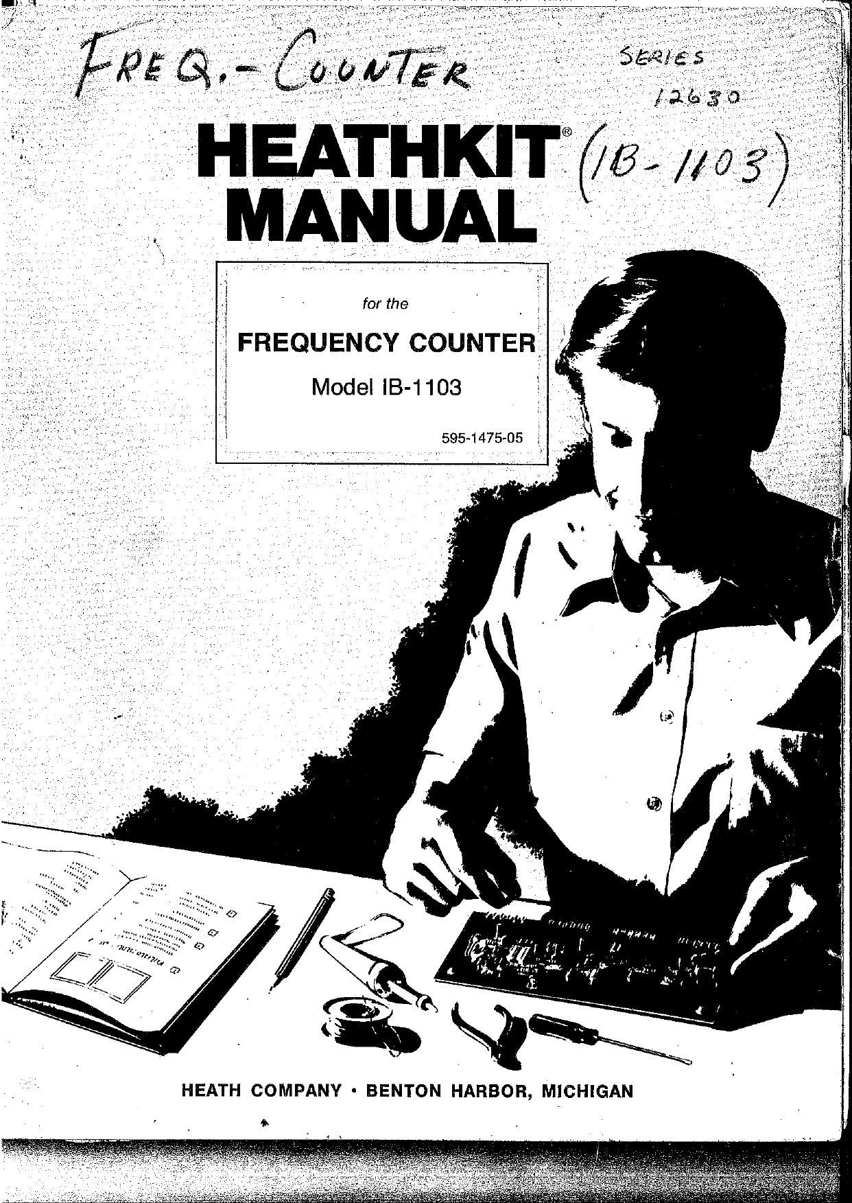
Heathkit IB 1103 Manual

This is the 32 pages manual for Heathkit IB 1103 Manual.
Read or download the pdf for free. If you want to contribute, please mail your pdfs to info@audioservicemanuals.com.

Page: 1 / 32
left right
Heathkit IB 1103 Manual

Extracted text from Heathkit IB 1103 Manual (Ocr-read)


Page 1

MANUAL

for the

i
i
_, 1 FREQUENCY COUNTER
1 Model IB- 1103

595-1475-05

.3


HEATH COMPANY - BENTON HARBOR, MICHIGAN

A

Page 2

Prlce $2.00

Heathkit® Manual

- for the

FREQUENCY COUNTER
Model IB-1103

595~1475-05

_.-¢_.4

Copyrlgm © I973
Heath Company

H E AT H C O M PA N Y All nghts Reserved
BENTON HARBOR. MICH'GAN 490 2 2 Printed In the Unlled Shams oi Amsvlca

Page 8

Page 90

SAMPLE TEST CHART ' '

Learn how to use the following "Troubleshooting Charts,
by referring to the Sample Test Chart below and reading
through the following paragraphs. Do not actually perform
the steps. The numbered paragraphs below are keyed to the
circled numbers on the chart. .

® Turn the Counter Off or On, as instructed here, with
the On-Off switch. WARNING: Always turn the
Counter Off when you remove or install lCs. When
you remove or install any other component, always
unplug the line cord, as line voltage is present at a
number of points in the chassis as shown by the
boxed-in areas in the Chassis Photographs" on Page

_HEATI-IKIT@

Follow the instructions given here before you perform
the test.

@ This is the test result.

As a step is performed, you will get a YES or NO result (or
other instruction), which steers you to the next step. These
steps will quickly bring you to a point where you are
instructed to check a particular component. Check the
component for proper installation. Replace the component
if it is faulty.

After a repair has been made, check the Counter for proper
operation, or follow the instructions in the step on the Chart
where the fault first showed up. If the kit still does not
perform properly, return to the beginning of the Chart and
begin the tests again. POssibly there is more than one
problem that must be corrected.

Do Not Use This Sample
Test Chart for Any Tests

107.
ON/OFF
STEP SWITCH
NO- POSITION
, arr
@ Remove R524 and R525.
/yv0N

Display indicates 100.0 Hz,
@
ON/OFF I '
SWITCH |
POSITION l
l
l
l
lJlll
Check 0511.

[JFF

Replace ICEOQ.

_I-IE1.AIII-IKIT@
FREQUENCY MU LTIPLIER TROUBLESHOOTING

( ) See the "Sample Test Chart" on Page 90 before
proceeding.

( ) Apply a 100 Hz input signal to the input of the
Counter.

( ) Position the front and rear panel switches as follows:

FRONT PANEL REAR PANEL
On/Off IN OSC INT
1 SEC IN

X10 |N

Frequency Multiplier Chart #1

0rr

Remove R524 and R525.
0N

Display indicates 1000 Hz.

Check 0511, 0509, and 10508 gate C. After repairing, reinstall
resistor R524 and R525

<
r11
YI-
-

'Page 91

l 1 Check the power supply voltages at J5. See Power
Supply Check" on the fold-out from Page 80.

l l Turn off the Counter and disconnect the input signal.
( ) Turn the Counter on and watch the UNLK lamp.

( ) Reconnect the 100 Hz input signal and watch the
UN LK lamp.

( ) If the UNLK lamp is off but was on when there was
no input signal, proceed to Frequency Multiplier
Chart #1." if the UNLK lamp is on and does not turn
off, proceed to Frequency Multiplier Chart #2.

OFF

E> Replace 10509. Also reinstall resistors R524 and R525.

Page 15

Page 102

r

|C401 is an operational amplifier that senses the average
voltages at the inputs to the Schmitt trigger. It then adjusts
the bias on transistor 0406 to equalize the input. to the
Schmitt trigger.

The TTL (transistor transistor logic) GATE pulse from the
time base circuit board is changed to ECL levels by resistors
R434 and R435. Section C of 10403 and FFB of |C402
improve the rise and fall times and invert the GATE pulse.
The inverted GATE pulse goes to the gated multiplexer and
turns it on and off at the proper times.

There are two outputs from the Schmitt trigger 0402).
The 0 output goes to Section A of |C403, which serves as a
line driver to the frequency multiplier. The 0 output of
|C402, FFA, goes to Section A of |C404. If the multiplier
circuit is activated, the multiplied output from ICSOQB
comes into Section B of lC404. Section C of |C404 enables
either Section A or Section B of lC404, depending on the
status of the multiplexer control input (pin 9). The outputs
of Sections A and B of lC4D4 of the gated multiplexer go to
the first decade counter. The outputs of the first decade
counter are then applied to differential level translators,
which convert the ECL levels to TTL levels, to drive the
following logic on the counter circuit board.

COUNTER CIRCUIT BOARD

The A, B, C, and D line signals, which represent 1-2-4-8 BCD
(binary coded decimal), from the input circuit board are
connected to |C102, a buffer/storage unit. During the
transfer pulse from the time base circuit board, which is
amplified by transistor 0101, the 1-2-4-8 information is
stored in ICIOZ. Then decoder/driver lC103 decodes the
1~2-4-8 into decimal and grounds the proper cathode of
display tube V1. The cathode then glows and displays a
number.

During the counting time, the signal to pin 2 of |C102 is also
used as the carry and drives the next decade counter, |C101
and lCiO4. |C101 divides by two and |C104 is connected to
divide by five. The following counters then each divide the
carry signals they receive by 10. The buffer/storage,
decoder/driver, and display tubes function as previously
described. During the reset pulse, all the decade counters are
returned to 0. The selected decimal point in the display tube
is connected through the switching system to ground.

The last carry pulse is applied to the cloek input of FFA of
[0125, as shown in Figure 12. The flip-flop changes state
and the 0 output is applied to the clock input of FFB of
|0125 and the D input of FFA of |C126. When the transfer

-HEATHKITe
+100v
R112
+5v
R111 1..
LAMP OVER
0104 0103
R108
R109
5
IC12o Q iClZfi c
FFA FFB
CL0C1< D CLOCK D
TRANSFER 3 2 11 12
12 9
1C125 L) 10125 0
FFA FFB V
CLOCK CLEAR CLOCK CLEAR
CARRY 1 2 5 e

7 TO 1C101
RESET R106 0102

Figure 12

pulse arrives at this clock input, the 0 output goes high and
turns on 0104 and the "l" lamp. However, if the input
frequency is so high that another carry pulse arrives before
the transfer pulse, the 0 output of FFA of lC125 will go
low and the 0 output of FFB of |C125 will go high. In this
condition, when the transfer pulse arrives only the Over"
lamp will be turned on. Then the reset pulse triggers 0102,
and lC125 is cleared for the next count. The reset pulse also
clears [0101.

TIME BASE CIRCUIT BOARD

The 4 MHz clock signal is divided by 4 and applied to the
INT-EXT switch on the rear panel. The selected clock
signal is then divided by either one thousand, one hundred
thousand, or one million by the following decade counters.
If the division is by one million, the multiplexer (a
digitally-programmable switch), |C207, is in the position
shown. if the division is by one thousand or one hundred
thousand, time base switches are in one of the other
positions and decade counters |C201, lCZO2, and possibly
l0203 are out of the circuit.

-I-IEATI-Ixrm

1 100 201)
I

k-T-v

1C 210 $-
FFA ,7
plN 12 -lsec

Page 103

300 400 500msrc
I

l
:«1 +1

F1

lflflmsec, or imsec

SPEED-UP
1C21o
FLIP-FLOP FFB
PIN 9

TRANSFER 'C209
PINS

lODusec

RESET |0209
PIN 5

iUOpSEC

|CZO9
H0
LD PIN b

RESETS ALL DECADE COUNTERS

ON TIM

MONOSTABLE ICZOB
MULTIVIBRATOR PIN 8

15nse:

.1

TL; 5 200msec

E BASE CIRCUIT BOARD 10 1

Figure 13

Consider the multiplexer to be in the 1 kHz position as
shown in the Schematic. The D output from |C204 is then 1
Hz. FFA of lC210 then further divides this signal to produce
a one-second pulse as shown in Figure 13. As the one-second
pulse is completed, the trailing edge of the pulse triggers
FFB of |C210, the speed-up flip-flop. The output of FFB
reprograms the multiplexer (at input C) to the 1 MHz
position and decade counters |C206 through |CZO4 divide
the signal. Because the GATE pulse is now low, the decoder
(IC209) is uninhibited and starts decoding its A, B, and C
input lines. The result is first, a transfer pulse from pin 3'
second, a reset pulse from pin 5; and third, a pulse from piri
6 that clears the speed-up flip-flop. As the speed-up flip-flop
clears, the multiplexer is switched back to its original
position and the monostable multivibrator (IC208) is

started. This monostable sets the six decade counters to 9.
At the end of the monostable pulse, the first pulse from the
clock starts the one-second GATE pulse again.

Decoder

The decoder, |0209, requires a negative pulse at its D (pin
12).1nput before it will decode. Therefore, it is inhibited
during the one second positive GATE pulse.

Multiplexer

The strobe input (pin 7) is always at ground. Because it is
not used in switching, it will be ignored in the following
description of an equivalent circuit.